|
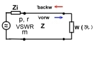
Using the Smith chart.
In this article no software programs are used. This gives a better understanding of
what the computer does when you work with a Smith chart program. The Smith chart makes it possible to view many parameters at different frequencies at once. These parameters are:
English  German German 
- Impedance: W Scheinwiderstand
- Resistance: R Wirkwiderstand
- Reactance: X Blindwiderstand
- Admittances: Y Scheinleitwert
- Subceptance: B Blindleitwert
- Conductance: G Leitwert
- Line length /Wave length : l/Lambda . Lamda = c/f. Leitungslänge / Lamda
- Reflection angel: deg. Winkel der reflection
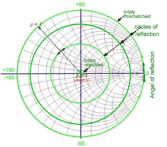
- Reflection :
 =S11= S22= p= r, Reflexion =S11= S22= p= r, Reflexion
-
Transformer ratio : n, r, ü Übersetzungsverhältnis
Impedance and Admittance smith chart.
Fig.1 shows a simplified smith chart for Impedances. An impedance point somewhere in the chart is defined as:  The numbers in the table are displayed as normalized values of W / Z.
Z can be selected freely: It is helpful to keep in mind that with discrete components, series inductance has positive reactance, while a series capacitor has a negative reactance: The numbers in the table are displayed as normalized values of W / Z.
Z can be selected freely: It is helpful to keep in mind that with discrete components, series inductance has positive reactance, while a series capacitor has a negative reactance:
Fig.2 shows a simplified smith chart for Admittances. A point somewhere in the chart is defined as:  The numbers
in the chart are shown as normalized values Y*Z. It is helpful to keep in mind that for discrete components, parallel capacitor
has positive reactance, while a parallel inductor has a negative reactance: The numbers
in the chart are shown as normalized values Y*Z. It is helpful to keep in mind that for discrete components, parallel capacitor
has positive reactance, while a parallel inductor has a negative reactance:
For strip lines and wave guides the reactance X and subceptance B depends from the mechanical design. For instance: Short stub wave lines can be positive or negative.
Fig.1 Smith chart for impedances without wave length scale. Fig.2 Smith chart for admittances without wave length scale.
One of the important thing while working with the smith chart, is to change from impdance values to admittance values and vice
versa.To implement this change of impedance to admittance to overlap some electronics developers, the impedance and admittance diagram. This may be somewhat confusing as Fig.4 shows . Another option is to work in the impedance diagram and change to admittance as follows: The admittance point is at 180-degrees on the same reflection circle as Fig . 3 shows.
The change from admittance to impedance is vice versa.
We always must know, what we just use, the impedance chart, or the admittance chart.
Lets write a normalized impedance W in the chart::
- We write in Fig3 and in Fig.4 : W= 0.6 + j1.2
- We find : G = 0.33-j0.66. At Fig.4 the point W becomes G but keeps on its place, the scales changes.
 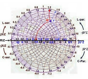
Fig.4 Impedance and Admittance chart overlaps.
Fig.3 The change of impedance to admittance diagram and vice versa
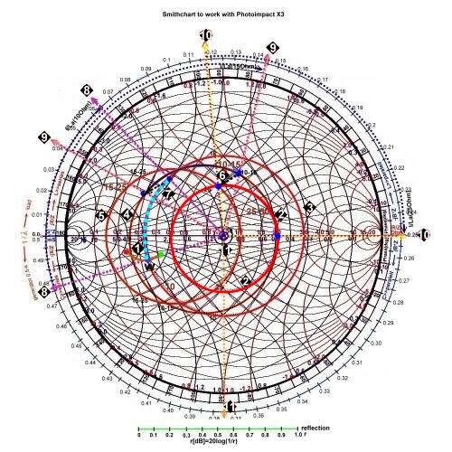
Now we use the total chart inclusive wavelength, and phase and reflection scale: Fig.5
- r = 0.63 , angel = 71.5 deg.
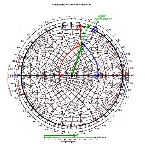 Fig.5 reading of the reflection values Fig.5 reading of the reflection values
- S11 = 20log(1/0.63) = 4dB
- VSWR = 4.44
So far we have not looked for normalization of the W point. If we would
have normalized W to 50 ohms, the circuit value would be :
,
- Wcircuit =Wchart*50 = 30+j60
- F=100Mhz : R=20Ohm; in series with L=95.5nH;
The admittance point has a a circuit value of :
- Gcircuit = Gchart/Z= 0.0066-j0.0132
- At f =100MHz the circuit could be: R=151 Ohm parallel with L=119.3 nH or 30Ohm in series with L=21nH.
Working with the impedance - admittance Smith chart, in a graphic software
.
In the following examples, we will use the simplified chart of Fig.00 (to the right >>>>>>>>) in a graphic software for instance photo impact X3, and a pocket computer. This simplified view is a rough diagram of overlook-planning . Here we
can use points, lines and circles in different colors, to realize complex broadband matching networks .
While working, we must always know what type of chart we use just the moment to focus on this chart. The graphics charts
on this site may be copied directly to be used with "zoom 100" in a graphics program.
. On the bottom of the chart is the reflection scale r. Other values values can be calculated from:
- Reflection: p = = r, r/dB = 20log(1/r):
- S-parameter S11, S22 = r [< grad]
- Matching factor: m=1/VSWR, m=(1-r)/(1+r);
- Ripple factor VSWR= (1+r)/(1-r);
- Maximum ripple due of reflection: a < -10*log(1-r*r) = (-ln(sqr(1-r*r))*8.7
.
During the design of circuits with the Smith chart, there seems to be always many solutions, but not all of these solutions are
acceptable. To keep the order during the work, I use a solution tree and write down and save all the roads that I've been trying to get a solution.
Transformers in the Smith Chart.
The next item to learn is the use of transformers in the smith chart. The transformer ratio of resistors and of complex resistors
is is square of the transformer voltage ratio n
- Vout / Vin =n
- Xout/Xin = n*n;
- Rout/Rin = n*n
Using a transformer in the chart, means, a point W is moving the factor n*n on the R/Z scale. In case of n=1,42; n*n =2 and W/Z=1+j0.1 the transformed impedance is W/Z=2+j 0,2. This is true too for tapped coils.
Wave lines in the Smith chart.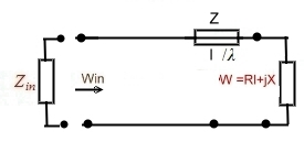 . .
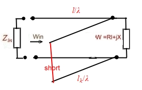
Fig.1 Impedance and 75 Ohm line
We want to find the value of an impedance, connected by a wave line of 75Ohm.
The frequency is 1GHz and epsilon of the wave line is 1. Fig.2 shows the arrangement. If we have for example an impedance at a certain frequency of :
W = 100 + j80.
We first must normalize the values to 75 Ohm .We get :
W/75 = 1.33+j1.06.
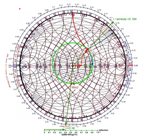
Now we will it into the chart. To normalize with 75 ohms means the center of the Smith-chart R/Z=1 on the real line is 75Ohm. Now we go along this line (red) to the R/Z value of 1.33. Next is to go up along the reactance circle of 1.33 to the X/Z value of 1.06. Thats the point of W in Fig.1. Now we can see how match is the reflection. The reflection is the radius of a circle around the point R/Z=1. (green circle) Every point on this circle has the same reflection. Using the reflection scale at the
bottom of the chart, we read a value of reflection of : r = 0.42,, this means r = 20log(1/0.42) = 7.35 dB,; angel = 48deg. Finding of the admittance-value Y of W is very easy , we focus on the admittance chart and find in Fig.1: Y*Z=0.47-j0.36 . Now we connect W with a 75 ohm line with a wave length of 30 cm and epsilon = 1.(Fig.2) to the input. We calculate from the frequency : lamda=c/1Ghz; l =30cm, l/ lambda = 0.2 . We go straight from W to the outer wavelength scale and find the point: l/ lambda=0.184.
This wavelength becomes clockwise (waves from the load to the generator) +0.2 greater and we get l/lamba = 0.384.Win now is on the straight line on the reflection circle of W. Win/75 = 0.78-j0.69. The length: l=0.384*30cm =10.44
Fig.2 Example of wave line and reflection
using the impedance chart.
Now we have to clarify the length of the wave line. We have epsilon =1 and l=30cm, but what will be the length x of the wave
line if epsilon has some other value? If epsilon increases, the wave line must be longer.
The following formula is valid :  . .
If for instance epsilon is 2.o5 of Teflon, the mechanical length will become: lx=10.44*1.43 =14.92cm
In Fig1 a load W is connected via one wave line having a certain Z. We could use more than one wave line in the series which
have different impedances as Fig.3 shows. Lets look on an example: Fig.3 Different wave line
impedances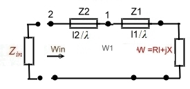
- Zin=75.
- W=100+ j80
- Z1= 240Ohm, l/Lambda =0.1
- Z2 = 75 Ohm, l/Lambda =0.1
- First, we think us point 1 open , now we have the same situation as in Fig.1 and we normalize to 240 Ohm :
- W/240 =0.41+j0.33 then twisting l/lambda = 0.1 and find:
- W1/Z=0.94+j1.01.
- W1circuit=W1*240=225.6+j242.4.
- We normalize this values to 75 Ohm :
- W1circuit/75 =3.0+j3.24, then twisting l/lambda = 0.1 and find:
- Win/75=0.698-j1.81
- Wincircuit=52.3-j135.7
We see different line impedances in series, causing a jump of W or Y values.
Different strip line impedances, therefore are often used to match Impedance's. In
the above example, we looked to the load, so we had to increase the wavelength in the clockwise direction. In the case of known Win, looking from point 1, we need to rotate counterclockwise.
Equations for series wave line mechanical dimensions, can be found at:
Passive and active Microwave circuits J.H.Helszain Wiley
Up to now, we used the wave line as Impedance's.  We also can use a wave line as an admittances in a parallel circuit . We also can use a wave line as an admittances in a parallel circuit .
For instance a short stub. Fig.4. Using the Formula for W we work
directly in the impedance chart:
Fig.4 short stub The general formula of a stub is : >>>
As it is known, there many circuits for paralleled wave lines:
- Open mode
- Shorted mode
- Loaded mode
In these cases, we can calculate the admittance or impedance values from formulas : Go to loaded wave lines formulas
Then write the susceptances or impedance values into the Smith Chart and add it to other values. Important is the paralleled
short stub where the reactance is: 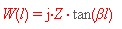 Changing from W to the admittance chart gives us the values of B to be added: For instance we have l/lambda = 0.204 and a short what makes R=infinit and and Z=1Ohm we get : jX=3.3 and jB=0.3 using a Z=25 Ohm line, we get : jX=82.5 and jB=0.012 Changing from W to the admittance chart gives us the values of B to be added: For instance we have l/lambda = 0.204 and a short what makes R=infinit and and Z=1Ohm we get : jX=3.3 and jB=0.3 using a Z=25 Ohm line, we get : jX=82.5 and jB=0.012
Admittances of short stubs are an important tool in the highest frequency technology. At microwaves, they have the advantage
of easy tuning of matching using little paralleled screws, holes, or irises. But watch out for broadband applications, the
impedances of the short stubs are repeated with the frequency due to the tangent formula.
Formulas for B of wave guides can be found at:
Journal of applied physics 18/ 1997
Holzain passive and active microwave circuits
The paralell resonator in the smith chart.
Resonators are very useful for broadband matching using the Smith Chart.
Look the resonator at Fig.1. Ro represents the losses from the unloaded Q. Q can be loaded with a additional external resistor Re to be used for matching. Rp=Ro//Re and QLOADED=Rp/(wo*L).
. 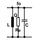 Practical Formulas of a lumped paralleled resonator in the smith chart are:
Fig.1 Resonator used for matching Practical Formulas of a lumped paralleled resonator in the smith chart are:
Fig.1 Resonator used for matching
:
We have found, that the conductance comes from Rp . The susceptance depends (14) on L, whose values are changed at higher frequencies by the parasitic elements.
If we normalize with Z for working in the chart , the normalized conductance will become Rp*Z (6) and the susceptance B depends on the detuning v and from its sign.: Therefore adjusting Rp and v, total of
admittance changes.(10).This is helpful to adjust a matching circuit.
Fig.2 Parallel resonators in the admittance smith chart .m
Now let's make an example for for = 700 MHz:
- L= 30nH; C=1.7pF;
- Q=1.89;
- Ro = 3500;
- Re = 268; to load Q;
- Rp = 250;
- Zo =50; 1/Ro =4mS; Z/Ro =0.2 ;
Reading the point pk : Y=0.2-j0.5 ; Y/50 = 4mS-j10mS; B=-j10mS; looking for the frequency with: v =B/(Q/Rp):
- The detuning is : -v =10mS/(1.89/250) =1.322 using (11) we get : f- = 377Mhz
- for the same positive detuning we have: f+ = 1300Mhz
 Fig.3 Parallel resonator circles in the impedance smith chart. Fig.3 Parallel resonator circles in the impedance smith chart.
Summarizing :
- The parallel resonator circles, are are the same circles as the conductance G circles in the admittance chart.
- Resonance frequency fo is is on the real scale. R/Z=Rp/Z.
- The subceptance is depending from: fo, L and v .
- The parallel resonator has 4 parameters to adjust for matching : fo,L,v and Rp.
Changing from the admittance chart to the impedance chart, we find
the impedance circle of the parallel resonator Fig.3 This is important when we add any other impedance. We see, the circles and the point
pk and the direction of the detuning keeps on the same location, but pk now is an impedance having other values. We will get the same result using the well known formula for the
parallel resonator  Using a little computer program for this formula , which changes to polar coordinates adding phase and vector , we can directly go to the impedance smith chart. Using a little computer program for this formula , which changes to polar coordinates adding phase and vector , we can directly go to the impedance smith chart.
W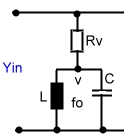 e have found the Impedance of the parallel resonator. Yet we e have found the Impedance of the parallel resonator. Yet we 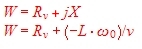 could add a series resistor to the resonator Fig.4 and shift the circle along the real line. The following formula is valid for high Q resonators : could add a series resistor to the resonator Fig.4 and shift the circle along the real line. The following formula is valid for high Q resonators :
Connecting a series resistor of 50 Ohm to the circuit of Fig.1 shifts the point pk near to the middle, as
Fig.5 shows 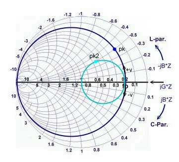
Fig.4 Paralell resonator and series resistor
Fig.5 Example 50Ohm and 700Mhz resonator
The series resonator in the smith chart.
. To find the circles of the series resonator, we begin in the impedance chart and the circuit of Figure 4.
Here we have the resistor Rs from the loaded Q, and the following formulas: To find the circles of the series resonator, we begin in the impedance chart and the circuit of Figure 4.
Here we have the resistor Rs from the loaded Q, and the following formulas: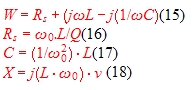 Rs=Ro+Re; Rs=Ro+Re;
Fig 4 Series resonator circuit
The circles of the series resonator are jX(v)/Z circles of a constant Rs/Z Fig.5.
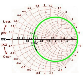 Fig.5 Series resonator circle in the
impedance chart Fig.5 Series resonator circle in the
impedance chart
The wave guide resonator in the smith chart.
Wave guide resonators can be considered as resonators of discrete elements to be analyzed in the smith chart, in the following way:
- Compute the losses from the cavity dimension as parallel resistance Rp see : Dr. Henne Höchstfrequenztechnik
- Measure the bandwidth b with an analyzer and compute the quality of the resonator Q=fo/b
- Compute : jB=(Q/Ro)*v; v=detuning
- Normalize to : Z= Impedance of the wave guide,
- Draw Rp/Z and B*Z(v) into an admittance smith chart.
- Change to the impedance chart.
Formulas to describe a wave guide resonator with lumped circuit elements, depending on the type of the shaft can be found in:
Gobau, Electromagnetic. Wave Guides and Cavities. (Pergamon Press ...1961)
Electronic matching , using the smith chart 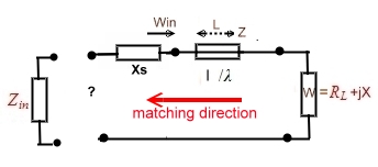 . .
Fig.1 Matching from the load to the input.
We look to the example of Fig.1 and say Zin is the output of a
coaxial connector of an electronic unit having Zin = 60 Ohm . Our goal is to match the impedance of W by another device, to minimize reflection .That means, Ro must be somehow by means of
impedances , and admittances or/and wavelines, brought to, or near the point 1, which is the normalized 60 Ohm point.This is the
way of matching electronic circuits, components, inputs and outputs to a real standard value, such as a cable or a filter with a specified value of reflection. This specification would be an other small circle around the R/Z =1 Ohm point.
At W/Z = f (f) over a frequency band, one can find each value of W/Z at a certain frequency in the same manner.We can either begin
matching with the impedance chart, or begin with the admittance chart.. There is is a practical rule for matching:
- Matching design begins on the load W , then matching to the input .
- Matching design begins on the input , then matching to the load W.
- Matching design begins on the input and the output.
Now we try to match W to the input Zin, using several examples:
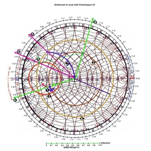
Matching Example #1:
We match the point W1 of Fig.2, which is the output impedance of a MOSFET transistor at 500 MHz , to a 100 Ohm strip
line of a printed circuit board:
 1; W1 is on the 100Ohm impedance chart. 1; W1 is on the 100Ohm impedance chart.
- 2; Change to the admittance chart.
- 2; Use an susceptance jB*Z= 0.38-0.15=0.23; along the conductance line to the G=1 line..
- 3; Change to the impedance chart.
- 3; Use an reactance jX/Z =2.55 ; along the R=1 line:
- Compute : B=0.23/100 , B=omega*Cp; Cp=0.23/(500E6*6.28*100) =0.7pF
- Compute : X=2.55*100; X=1/(omega*Cs), Cs=1/(100*2.55*500E6) =1.25pF
Matching Example #2: 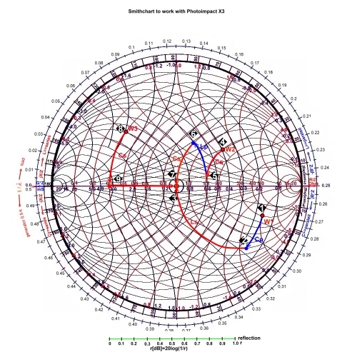 Fig.2 Matching examples Fig.2 Matching examples
We match the point, W3, who is the input impedance of an RF transistor at 100 MHz
Fig.1, to a 300 ohm antenna input.
- 8; W3 is on the 300 Ohm
impedance chart .
- Using a series capacitor, shifts W3 along the R/300=0.3 circle to the real axis.
- 9; -jX=0.4; Cs=13.2pF;.
- Next work, is a jump, using an RF-transformer from R= 0,3 to 1.
- 7 ;The ratio is Rout/Rin = n*n;
n=sqr(1*300/0.3*300)=1.8;.
Matching Example #3:
We match the point W2, which is the input impedance of an RF component, at 200 MHz to a 50 ohm coaxial input.
- 4; W2 is on a 50 Ohm
impedance chart.
- Due of DC Blocking, the matching circuit must have a series capacitor.
- 5; We stay on the impedance
chart, and go along the R=1.6 Ohm circle from -jX/50=1.2-0.29=0.94,
- This C can be realized by means of a series capacitor C=16.9pF
- 6; Changing to the admittance chart and going up along -jB*Z until the R/Z=1 constant circle, is met.
- The value -jB*50=0.49-0.1=0.39. The parallel L is: L=1/(f*6.28*0.0078) =102nH;
- 7; Next is a series capacitor C=19.9pF having a -jX/50=0.8 along the -jX/Z circle down to R/Z=1-->50Ohm;
Matching Example #4 : Matching of a transmitter power transistor:
Fig.1 C-Transmitter stage matching 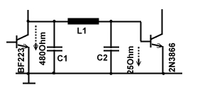
A classical transistor B or C power stage has not only to be matched, the
matching circuit must have a transmitter tank, having a loaded Q of 5..10. The input of an output stage is matched using a Collins filter as a tank, Fig.1, between two transistors.
We have: f=150Mhz, R1= 480 Ohm , R2=25 and use QL=5; C1must be 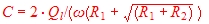 C1=18pF, C1=18pF,
Normalizing to 25 Ohm we get: 480/25=19.2 . deltaBC1*25
=0.423; The other values are taken from the smith chart of Fig.2:
 1 Basis input resistor : R/Z=19.2. 1 Basis input resistor : R/Z=19.2.- 2 C1 tank capacitor: 18pF.
- 3 Series-L1= 76nH.
- 4 Basis capacitor C2=59pF.
- 5 Collector output resistor: R/Z=1
>>25Ohm.
Fig.2 Collins filter
Matching-Example #5 : Matching of Impedances using only one Wave line.
Inside two circles in a smith chart of Fig.1 are the values of possible impedances W which can be matched with one wave
line to Zin. The length and Zo of the transforming line are matching parameters. In this case, the smith chart is not necessary , when the following formulas are used:
Fig.2 Equation to calculate a matching line 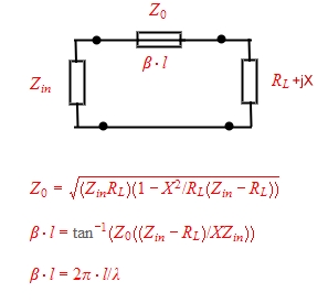 Fig.1 One line matching circles in the smith chart Fig.1 One line matching circles in the smith chart
Matching-example #6: Matching direction from input and from the output.
Sometimes it is helpful to match from the load side and work matching from the entrance at the same time. The input Zin,
normally is a normalized impedance which is represented in the chart as R/Z=1, r=0. This is the target for the transformation of
Wload when designing a matching circuit. From now on we use the circuit of Figure 1, in order to realize a new entrance with a
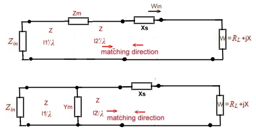
reflection of r =-Ym / (Ym + 2 (1 / Z). This is a new circle around G*Z=1. The matching circuit has to meet not only the single point 1, but it is enough the green circle somewhere to meet. Abb.2 1 After that, we can read from the outer scale, what the
necessary wave length, is to reach G = 1, along a B or X circle2
.
Fig.1 Matching from the input and from the output
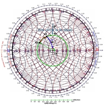
We repeat using Ym:
- 1 Use the admittance smith chart.
- 2 Estimate a practical reflection r circle aground G=1.
- 3 Compute the necessary Ym (stub)
- 4 Design a matching circuit from the load W to match
some where the reflection circle.
- 5 Read the l1/lamba from the smith chart scale along the circle.
- 6 Chose a practical value for 12/lamda.
- 7 Compute the wave line or wave guide length11 and l2.
In the same manner, the Impedance circuit of Fig.1 can be used.
The radius of the reflection circle is: r=Zm/(Zm+2Z).
Fig.2 Matching from the input
Matching-example #7 : Matching of Impedances using several wave lines having different Z.
One method of matching is the use of several series connected wave lines, having different Impedances. This method is best solution at very high frequencies, when the use of lumped elements is not possible. We begin with Fig.1. We want to match
the output impedance of a microwave power transistor at 1.9Ghz, W=3.4-j0.13 to a 50-ohm input, with a reflection of at least 25 dB.
- 1 The point W1 is normalized from the Data book at 10 Ohm. While this example, we change the normalization step by step forward and backward.
- 2 First we match from the input using a wave line with Z=50 , from R/50=1 to a value of R / 50 = 2.
jX=0 we say. We choose a wave length of the 50 ohm line l /Lamba =1/8. The next action is drawing of a reflection circle around R /
50 = 2 . This is the circle to met if matching from the load side with a Z=25Ohm impedance which normalized to 50Ohm will jump from R / Z = 2 to 1.
- 3 Now we change the direction in which we adapt, working from the load and decide to use wave lines of 10-15-25
ohms, to to achieve the 25 ohms reflection circle. We don't care , about the necessary l/lambda values and draw a
normalized 10 Ohm reflection circle around R / 10=1where the the point W lies.
- 4 We draw a reflection circle of normalized 15 ohms from the normalized 10 ohms circle real values, by multiplying
with 10/15, moving to the left.
- 5 From this we draw an normalized 25 Ohm reflection circle from the real values of the 15 Ohm circle, multiplying
this circle with 15/25.
- 6 Now we must find two points where the 15 Ohm circle and the 25 Ohm circle follow the values
W25=W15*15/25.
- 7 The same we must do for the 10 and 15 Ohm circles.
- 11 from the 25 Ohm circle a 50 Ohm line transforms W=jX+0 direct to the center.
- As we have now the points on the reflection circles we can read from the chart :
- 8 10 Ohm circle : l/lambda =0.088.
- 9 15Ohm circle : l/lambda=0.104.
- 10 25 Ohm circle : l/lambda =0.132.
- 11 50 Ohm circle : l/lambda =0.125.
- From the frequency of W we can compute the length of the strip lines at epsilon=1.
- From the dielectric constant we gain the real length:
You can make a comprehension exercise and repeat the operation at 2 GHz of W (red) and 1.8 GHz (green) of W,
with the values from the length l , of the 1.9 GHz example, and see the reflection of the entire frequency band.
Fig.1 Matching with staggered Z
Matching -example #8: Matching with different Z and Capacitor.
Using staggered Z and SMD-capacitors simplifies matching. One way to adapt in this way is shown in Figure1 , using to two
wave lines, 10 and 50 ohm and a capacitor:
- 1 Draw the impedance W/10 in the chart .
- 2 Draw an reflection circle of W/10 around R=1.
- 3 Multiply this circle with the impedance ratio 10/50; and draw a Z=50 Ohm circle.
- 4 Go around with l/lambda on the 10 Ohm reflection circle and find a useful point. l/lambda=0.17
- 5 Transform this point with the impedance ratio and find a point on the 50 Ohm circle .
- 6 Go around with l/lambda on the 50 Ohm reflection circle until it crosses the R/Z=1circle. l/lambda=0.027
- 7 Take the difference of B to B=0; R/Z=1 on this circle and compute the parallel capacitor with deltaB*Z=2;
f=1.9Ghz >>>: Cp=2/(50*1.9E9*6.28)=3.35pF.
Fig.1 Staggered Z and capacitor combined
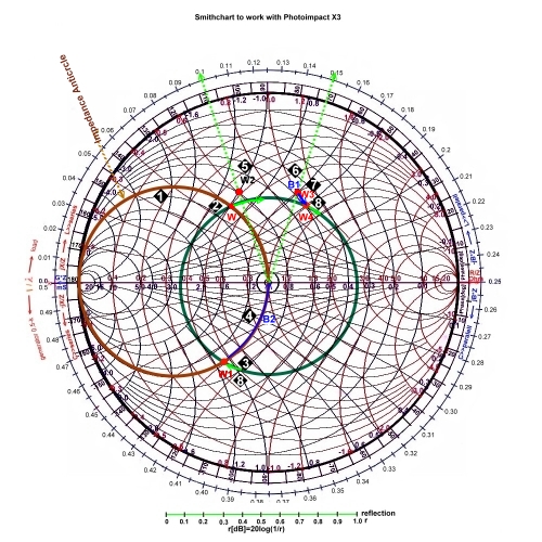
Matching-example #9: Using parallel stubs.
Matching by short stub was the classic method of adjustment, at a time, were not yet invented SMD capacitors.
Lets see how it works in Fig.1:
- 1 First do do is, drawing the anticircle.
- 2 The Impedance W=50+j50 shall be matched and brought to the point R/Z=1 for a normalizing Z of 100 Ohm .
- 3 Next is to use a quarter lambda line , to move the impedance W to W1 on the anti circle.
- 4 Jet a short stub having an -jB2*100 =1.1, shifts W1 to R/Z=1
Since this method is not operating in each point on the Smith chart, we can instead use two stubs:
- 5 The Impedance W2 shall be matched and brought to the point R/Z=1 for a normalizing Z of 100 Ohm .
- 6 First we use a wave line of l/lamba =0.05 and shift W2 to W3.
- 7 Now a short stub having an +jB1*100 =0.1 is shifting to W
- 8 Next is to use a quarter lamba line and shift the W to W1 directly on the antcircle.
- 4 Now a short stub having an -jB2*100 =1.1 shifts to W=100 Ohm;
Fig.1 Matching using parallel stubs.
Matching-example #10: Parallel resonator and series resonator as matching circuit.
Lets draw 2 circles into the smith chart , a parallel resonator circle (blue)1 and a series resonator circle (red)3 shown 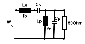 as a circuit at Fig.1. Both resonators have the same fo. We have: fo= 140MHz; Lp=53nH, Cp=11pF, Qp=100, Ro=4600,Qs=20. The blue circle of the parallel
resonator, with low losses, is almost identical with the outer B Circle. Paralleling the resonator and then 50 Ohm resistor does therefore not have any effect to the input resistor W at fo.2. The series resonator does transform the 50 Ohm
load to W=75 Ohm. The series resonator must have a value of 75-50=25 Ohm as a crossing point with the real axis.Then we must have : as a circuit at Fig.1. Both resonators have the same fo. We have: fo= 140MHz; Lp=53nH, Cp=11pF, Qp=100, Ro=4600,Qs=20. The blue circle of the parallel
resonator, with low losses, is almost identical with the outer B Circle. Paralleling the resonator and then 50 Ohm resistor does therefore not have any effect to the input resistor W at fo.2. The series resonator does transform the 50 Ohm
load to W=75 Ohm. The series resonator must have a value of 75-50=25 Ohm as a crossing point with the real axis.Then we must have :
Ls= Rs*Qs/wo =568nH. Fig.1, 2 Resonators for broadband matching
Fig.2 Resonators for broadband matching in the smith chart
Up to now, no reactances or susceptances are not used at all. In case of detuning the resonator, is it obvious, that the series
parallel resonator circuit will realize reactances or susceptances depending on the detuning v.
The matching in the impedance chart then can be written as: (normalized)
r = 0 ---->> W(v)/Z+Wresonator(v)/Z =1+j0.
.Now lets match a impedance W (f) using a series and parallel-resonator with high Q but different fo and v . First we look to
Fig.3 and find a transformer in the path. The design way is as follows:
- 1 The impedance W(f) to be matched to 50 Ohm
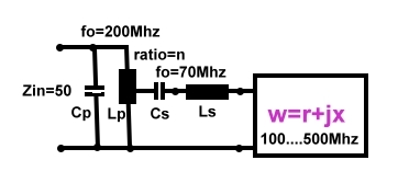
- 2 The impedance of a series resonator Wseries(v)
fo=70Mhz;Ls=10nH; Cs=517pF; Q=30; jXs/50=3E-03;
- 3 The impedance of added W(v)+Wseries(v)
- 5 The the admittance of a parallel resonator: Yp*Z(v),
fo=200MHz; L=117nH,Q=100; n=1.18;
- 4 The the impedance sum of:
(W(v)+Wseries(v))*n*n; ratio: n*n=1.4;
- 6 The impedance sum of :
(W(v)+Wseries(v))*n*n+Wparalell(v)
- Broadband reflection is r(100-500MHz) =16-24dB;
Fig.3 Series and parallel resonator matches transistor input impedance
Fig.4 resonator matching in the smith chart
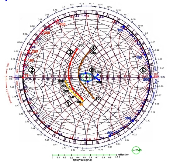
Matching-example #11: Very broadband constrained matching , using one LC resonator .
Here is an other example of broadband matching an Impedance to a 50Ohm input. The impedances to be matched over the
frequencies are typical for a bidirectional transistor 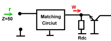 , to be used in a low Ohm input, base common circuit: Fig.1 , to be used in a low Ohm input, base common circuit: Fig.1
The values are:
- f= 200Mhz; W= 10+j0;
- f= 500MHz;W= 9+j6;
- f=800MHZ, W= 7.5+j13;
- f=1GHz; W= 5+j22.5;
Fig.1 Broadband matching common base Transistor
We normalize this datas to 50 Ohm and write the values into the impedance smith chart of Fig.1 1. The problem here is
the frequency range between 500MHz and 1 GHz, where wave lines are too long and lumped inductivitys have relatively low Q and low selfresonances. Additionally, PCB nodes have a 0.2 to 1 pF parasitic capacitance, therefore series resonators will
not work correctly. Lumped broadband transformers have high stray inductivity's in this frequency range and can not be used. The components which can only be used her are :
- SMD ceramic capapacitors.
- High Q air coils.
- Parallel resonators.
- SMD resistors.
Yet we want find a matching circuit using only this components.The entire system has a lot of gain, so we use 2 to 3 dB loss
for constraint-matching First is, that the node of the input has a parasitic capacitance. This is a parallel Cp to the input ,
therefore we must focus to the admittance chart . Here, we can see, that a parallel capacitor on the input is helpful for
matching, because it gives the transistor impedance W(f) a more circled shape. This is our matching goal, a small reflection
circle around R / Z = 1 -->50 ohms. First we try a 7pf parallel capacitor, at 4 and find it to large. Therefore we reduce the
parasitic capacitor to 1 pF, and add the admittance to the transistor admittance data2. Now we calculate to use a parallel resonator 5 for compensation of this values. We compute the following values to be drawn into the admittance smith chart:
|
F/MHz
|
v
|
jB*50
|
|
180
|
0
|
0
|
|
200
|
+0.21
|
0.185
|
|
500
|
+2.4
|
2.1
|
|
800
|
+4.2
|
3.7
|
|
1G
|
+5.3
|
4.7
|
|
- fo = 180 MHz;
- Q = 80;
- L= 50nH, C=15,6pF;
- jB= (1/wo*L)*v;
- v=(w/wo)-(wo/w);
We add the admittances of the resonator to the admittance values of curve, 2 but we find , that this is not very helpful,
because resistance transforming is missing. To get resistance transformation, and move W to the right , we connect a resistor of 45 Ohm parallel to the resonator. 6. Now we are concentrating on the impedance chart: We see, that to use the parallel resonator used as an series circuit can shift impedances near to the 50 Ohm point. Therefore we keep the parallel resonator ,
but in series as an impedance. To do this we let the circle6 as it is, focus on the impedance smith chart and add the values to 2. The result is 7 already a good matching. On a PCB circuit we will have a node at this point with a 0.2 to o.5 pF
parasitic capacitor. Therefore, we must go back to the admittance chart and add the parasitic's B values. This improves the reflection to r=20dB8. Fig.2 shows the simple circuit we have found , including the parasitic's
Fig.1 Broadband matching example
Fig.2 Broadband constrained matching circuit from Fig.1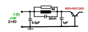
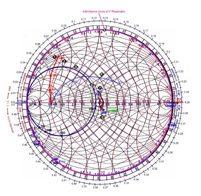
Matching-example #12: Lumped LC filter as as matching circuit.
In the example #10 a tapped coil is used in the matching circuit. Manufactured coil taps cannot reproduced precisely, tapped coils are therefore no longer used. In this example we want to match the Impedance of the above example without tapping, as an filter to reject the outside band . W(f)/Z--->> 1 :
|
PR
|
f/MHz
|
v
|
jB(f)*Z
|
|
fo=500MHz
|
100
|
-4.8
|
-0.85
|
|
Ls=90nH
|
150
|
-3.0
|
-0.53
|
|
Cp=1.1pF
|
200
|
-2.1
|
-0.37
|
|
Ql=50
|
350
|
-0.73
|
-0.13
|
|
Go*Z =0.0035
|
500
|
0
|
0
|
|
First we use a parallel resonator and add its susceptances B(f)*Z to the suceptances of W(f)/Z. Our goal is to move W(f)/Z into the direction of normalized 1 (50Ohm) and give this curve a circle shape, as small as possible.
Therefore we use, the following datas: :>>>
As Ro/50 = 188 the resonator susceptances lay on the outside circle.0 .We use
the admittance smith chard and add jB(f)*Z of W(f)/Z to B(f)*Z of PR an get 2.
|
SR
|
f/MHz
|
v
|
jX(f)/Z
|
|
|
70
|
0
|
0
|
|
fo=70MHz
|
100
|
+0.72
|
0.063
|
|
Ls=10nH
|
150
|
+1.67
|
0.14
|
|
Cs=517pF
|
200
|
+2.5
|
0.22
|
|
Ql=150
|
350
|
+4.8
|
0.42
|
|
Rs/Z=0.003
|
500
|
+7.0
|
0.61
|
|
Next work is to use a series resonator to get the curve more circled. After trying some series resonator values, we use: >>>
As Rs/50 = 0.01 the resonator reactances lay on the outside circle of the impedance chard. We add jX(f)/Z of 2 to X(f)/Z of SR an get 3.
|
PR
|
f/MHz
|
v
|
jB(f)*Z
|
|
fo=200MHz
|
100
|
-1.5
|
-0.74
|
|
Ls=80nH
|
150
|
-0.58
|
-0.28
|
|
Cp=7.9pF
|
200
|
0
|
0
|
|
Ql=50
|
350
|
+1.18
|
+0.58
|
|
Ro=5000
|
500
|
+2.1
|
1.0
|
|
Next work is to use a parallel resonator PR to get the curve closer to 1. After trying some resonator values, I used: >>>
As Ro/50 = 100 the resonator susceptances are on the outside circle.We use the
impedance smith chard and add jB(f)*Z of 3 to B(f)*Z of PR an get 4.
|
Ls
|
f/MHz
|
jX(f)/Z
|
|
|
100
|
+0.125
|
|
Ls=10nH
|
150
|
+0.18
|
|
|
200
|
+0-25
|
|
|
350
|
+0.43
|
|
|
500
|
+0.62
|
|
Next work is to use a series inductance to get the curve more circled. after trying
some values, we use: Ls =10nH, and calculate:>>>
We add jX(f)/Z of Ls to X(f)/Z of 4 and get 5.
N
|
Cp
|
f/MHz
|
jB(f)*Z
|
|
|
100
|
+0.21
|
|
|
150
|
+0.32
|
|
Cp=7pF
|
200
|
+0.43
|
|
|
350
|
+0.73
|
|
|
500
|
+1.1
|
|
ext work is to use a parallel capacitor to get the curve closer to 1. After trying some values, we use: Cp= 7pF and find:
>>>
We add jB(f)*Z of Cp to B(f)*Z of 5 and get 6. This curve now has symmetrical
positive and negative values; which can be compensated, using a series resonator having the same positive and negative values.
:
|
SR
|
f/MHz
|
v
|
jX(f)/Z
|
|
fo=230MHz
|
100
|
-1.86
|
-0.63
|
|
Ls=12nH
|
150
|
-0.88
|
-0.3
|
|
Cs=40pF
|
200
|
-0.28
|
-0.096
|
|
Ql=50
|
350
|
+0.86
|
+0.29
|
|
Rs=0.01
|
500
|
+1.7
|
+0.59
|
|
So we can write for this series resonator :
B*Z(+v) =(v+)*wo*Ls*Z = B*Z(-v)=(v-)*wo*Ls*Z
Solving the equation for a v of 100 and 500MHz gives fo and Ls:.
>>>
Now we add jB(f)*Z of Cp to B(f)*Z of 6 and get 7. This curve now is almost near 1: We find a reflection of 14 dB.
Last work is to use a little resistor of 4 Ohm get the curve ifen closer to 1. Fig.2 shows the result , we have now r=18dB. As this calculation is not very precisely , in a practical carefully tuned circuit, can the reflection be matched better than 20dB. Fig
3 shows the matching circuit.
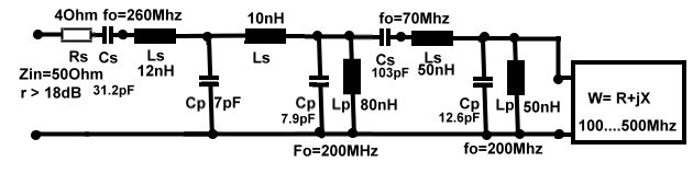
Fig.1 Broadband matching using a complex circuit
Fig.2 Matching filter
.Now we have roughly designed a very broad passband filter, where the complex impedance W is part of it . The frequency band with low reflection is the passband. Outside the low input reflection is the rejection band. The total filter transmission must
controlled in a transmission analyzing program, looking for all S parameters , improofing the circuit and then match again.
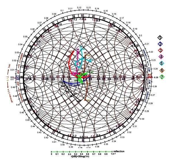
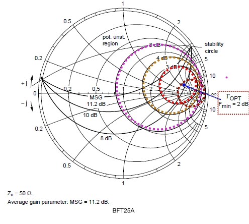
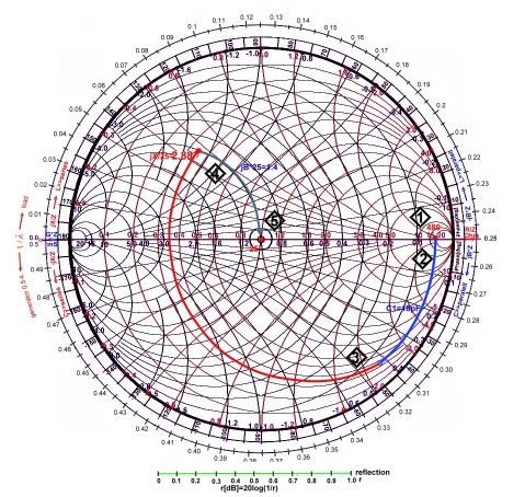
Matching example #13: Transistor matching using noise circles in the Smith Chart.
The smith chart is helpful for designing low noise circuits for low power low noise transistor amplifiers. Fig.1 shows the
situation at a certain frequency: Normally we take the transistor S parameters from the data sheet, and match the input and the
output of the transistor for stable maximum gain and minimum ripple in a way, that input and output reflection are as low as possible.
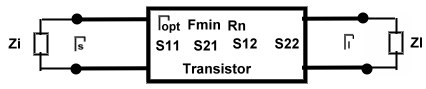 Fig.1 Low noise transistor matching Fig.1 Low noise transistor matching
For minimum noise the transistor input has to be matched with specified reflection  . But first we need to determine the the load reflection coefficient . So we
have to match the load impedance to S22 , and read . But first we need to determine the the load reflection coefficient . So we
have to match the load impedance to S22 , and read  in the Smith chart. in the Smith chart.
We then match the input for noise, using the following parameters:
- Minimum possible noise figure, at a certain frequency:
- Reflection coefficient of the noise minimum ,at a certain frequency:
- Minimum noise from the datasheet.
- Equivalent noise resistance.
The noise circles than can be computed using the following equations:
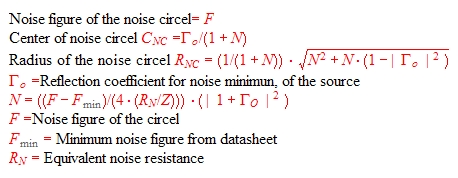
Normal , noise circles are given in the data sheets of transistors. Fig.1 shows an example of noise circles and . The noise circles are places for reflection ,at the the transistor input. To gain the wanted noise figure, must be inside the wanted F circle and then being matched to Zin . The noise circles are places for reflection ,at the the transistor input. To gain the wanted noise figure, must be inside the wanted F circle and then being matched to Zin .
Fig.2 Practical noise circles.
: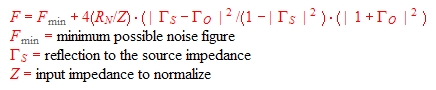 Once we have matched with a certain circuit, we can find the the noise figure belonging to this input reflection, using the following equation: Once we have matched with a certain circuit, we can find the the noise figure belonging to this input reflection, using the following equation:
We see, that the noise figure is minimum, in case of : =
The aim of the adaptation here is not only minimum reflection and minimum loss, but also minimum noise. The circuit that
matches the transistor input to a given impedance Zin of the input, must cause a compromise between S11, suitable for maximum gain and a usable from the noise circle of the transistor data sheet . One way to do this, is to design the
matching circuit in the following manner: Beginning matching to an input impedance value between S11 and of the noise circle as close as possible, and compute the belonging noise number from the formula of F.
Helpful is a small computer program, then enter the parameters and solve F very quickly in an iterative computation. In the same manner, the compromise
of overall gain, has to be calculated, with the gain formula and the load reflection :
: 
|
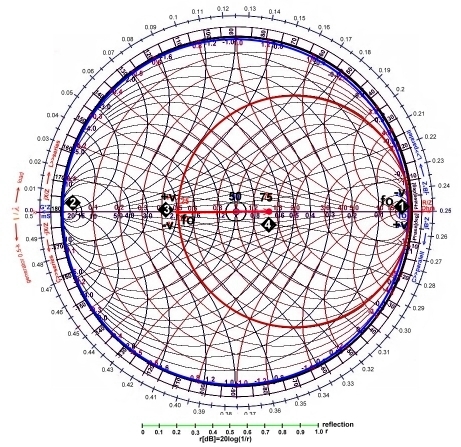
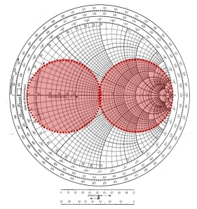
 The total reflection circle is the base circle of the Smith chart. Figure 1 shows the
reflection circles with Smith chart background. It is only the outer loop for the total reflection visible.The other reflection circles, are invisible,
and the designer must know that there are such circles. In Smith, paper charts are outside the circle, a reflection scale, either with r / dB or VSWR values. An other parameter depending from reflection is the
ratio of the voltages:
The total reflection circle is the base circle of the Smith chart. Figure 1 shows the
reflection circles with Smith chart background. It is only the outer loop for the total reflection visible.The other reflection circles, are invisible,
and the designer must know that there are such circles. In Smith, paper charts are outside the circle, a reflection scale, either with r / dB or VSWR values. An other parameter depending from reflection is the
ratio of the voltages: 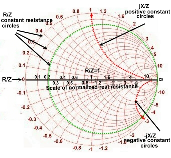 Here, the impedances in the Smith Chart are normalized to standard
impedances Zo or the input impedance Z . Then R=1 becomes Z.
Here, the impedances in the Smith Chart are normalized to standard
impedances Zo or the input impedance Z . Then R=1 becomes Z.